
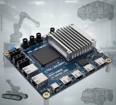
FPGA & SoC Implementation for High-Performance Systems
We engineer deterministic, timing-closed, production-grade FPGA and SoC designs that integrate compute, connectivity, memory, and firmware into a unified programmable architecture.
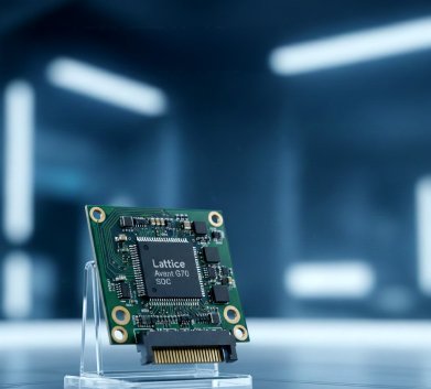
Our work spans architecture definition, resource partitioning, RTL development, timing closure, verification, and system bring-up — across Xilinx/AMD, Intel/Altera, Lattice, and custom SoCs.
DESIGN APPROACH DIAGRAM
A Structured, Architecture-First Approach to FPGA/SoC Design
Our methodology ensures clean architecture, efficient partitioning, and predictable implementation even in complex, high-speed systems.
System Requirements → Architecture Definition
- Workload characterization
- Latency & throughput constraints
- High-speed I/O requirements
Partitioning & Floorplanning
- Compute vs control vs pipeline
- Resource budgeting (LUT/BRAM/DSP)
- Clock & reset domain design
RTL Development & IP Integration
- Custom logic + standard interfaces
- PCIe/CXL, JESD204x, Ethernet, MIPI
- Simulation-first flow
Timing Closure & Implementation
- Constraint authoring (XDC, SDC)
- CDC/SDC checks
- Pipelining & retiming
System Bring-Up & Validation
- On-board tests
- Firmware integration
- Performance validation
TIMING CLOSURE PROCESS
Achieving Deterministic Timing at Scale
Timing closure is where high-performance systems succeed or fail. Our process is engineered
for predictable convergence across multi-clock, multi-interface designs.
Architecture & Partitioning
- Compute, memory, and interconnect planning
- FPGA/SoC partitioning (resources, clocks, resets, IP integration)
- BOM optimization and component selection
High-Speed Schematic Design
- PCIe Gen5/Gen6, CXL 3.0, JESD204x, MIPI, Display, Ethernet
- Multi-rail power domains and sequencing
- Clocking networks with jitter-constrained design
- Protection, isolation, redundancy design for mission-critical systems
PCB Layout & Routing
- Multi-layer HDI boards (10–20+ layers)
- High-speed differential routing (PCIe/CXL, SerDes, JESD, SATA)
- Length tuning & skew management
- Thermal mitigation & copper balancing
- EMI/EMC-aware layout best practices
SI/PI (Signal & Power Integrity)
- Pre-layout simulations (stack-up + constraints)
- Post-layout simulations for eye diagrams, return loss, crosstalk
- Power-delivery network (PDN) analysis
- Compliance preparation (PCIe, CXL, JESD, Display protocols, Avionics standards)
System Bring-Up & Validation
- Oscilloscope + logic analyzer based validation
- Firmware bootstrapping and diagnostics
- Thermal, environmental, and reliability testing
- Production test development
REPRESENTATIVE INTEGRATION CASES
Examples of firmware and embedded software powering Logic Fruit platforms.
PCIe Accelerator Board Bring-Up
What we delivered:
- PCIe endpoint firmware
- DMA driver + user-space API
- Diagnostics + performance test suite
Result:
- Stable, low-latency data paths enabling HPC and storage applications.
Embedded Linux for Autonomous Vision System
What we delivered:
- Custom device tree + drivers for multi-sensor pipeline
- Real-time ISP control software
- Edge inference module integration
Result:
- Deterministic perception-to-decision flow for robotics.
Firmware for Mission-Critical Display Chain
What we delivered:
- ARINC 818 / DVI protocol control firmware
- Display diagnostics + failover logic
- Thermal and status management
Result:
- Highly reliable avionics-grade display subsystem.
JESD204C Data Acquisition Firmware
What we delivered:
- JESD lane management & status control
- DMA + circular buffer software
- Runtime monitoring
Result:
- Stable multi-gigabit ADC capture for telecom and RF testing.
Partner with Us to Architect Your Next High-Performance System
Our architecture, schematic, layout, and SI/PI workflows are designed to accelerate time-to-market while delivering robust,
predictable system performance across compute-heavy and bandwidth-intensive applications.